
LTCC multilayer technology for demanding electronic applications
Ceramic substrates as circuit carriers for compact electronic assemblies enable demanding applications of circuits in areas such as power electronics, medical technology, industry and many more. Micro-Hybrid offers a comprehensive portfolio with LTCC and thick film hybrid technology.
Diesen Beitrag teilen

The choice of base material is of crucial importance within the designing process of electronic assemblies. High thermal conductivity, thermal resistance or mechanical stability are the basic functional requirements for the realization of electronic applications with concrete demands on long-term stability and reliability. For example, for applications in power electronics, the base material must have high thermal conductivity in order to dissipate the heat generated by the components quickly and efficiently from the conductive layers. This is ensured by the high thermal conductivity of ceramic substrates.
Applications for space and satellite technology require particularly high processing standards as they are exposed to high mechanical loads during launch. Likewise, the substrates and circuits must withstand the extreme environmental conditions such as vacuum, cosmic radiation and extreme temperatures in space during their mission time.
Micro-Hybrid Electronic offers thick film hybrid technology (based on Al2O3 alumina ceramic) and also LTCC technology to realize application specific circuits. Both technologies are especially suitable for such demanding applications due to the material properties of the used ceramics.
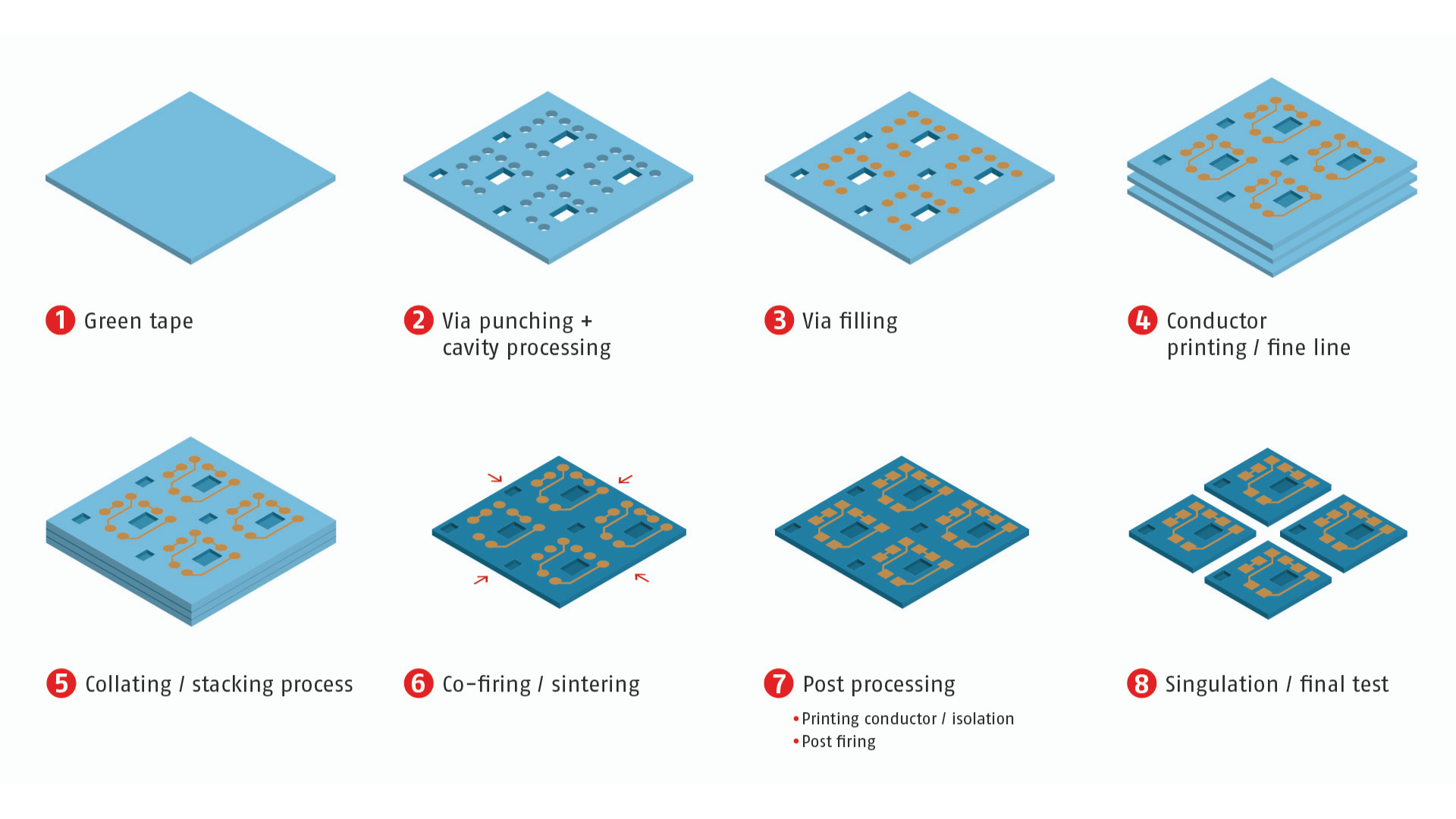
The production of LTCC or low temperature cofired ceramics based assemblies in our LTCC competence center is carried out according to customer requirements, from the development of the circuit layout to the in-house production of the specific LTCC substrates to the assembly of components, embedding of chips, chip and sensor modules as well as sealing by means of appropriate housings. As a rule, layer thicknesses of 40 to 200 µm per layer are used (others on request). Circuits from 3 up to 40 layers can be realized. However, the individual parameters of the application are always decisive for the circuit design. Our technology and electronics developers develop the optimal circuit design for this purpose.
The manufacturing process of the customer-specific LTCC substrates consists of 8 process steps from the green tape with 6" x 6" (unsintered), the punching of vias and cavities, their filling with metallic pastes to sintering and separation.
The results are ceramic circuit carriers with precisely adhered to application-specific specifications for further assembly and processing up to finally calibrated and tested assemblies and sensor modules.
Send us your inquiry.


